Addressed in this tutorial are common mode voltage range and common mode rejection as they pertain to instrumentation amplifiers, their architectures, and their applications.
Instrumentation amplifiers (in-amps) amplify the difference between two signals. These differential signals typically come from sensors such as resistive bridges or thermocouples. Figure 1 below shows a typical Instrumentation amplifier application where the differential voltage from a resistive bridge is amplified by the AD620, a low-power, low-cost integrated instrumentation amp.
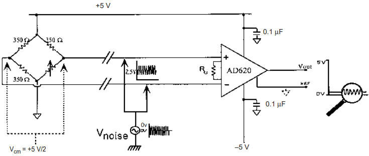
In thermocouple and bridge applications, the differential voltage is generally quite small (a few millivolts to tens of millivolts). However, the two voltages from the bridge are approximately 2.5 V when each is referenced to ground. This voltage, which is common to both inputs, is called the common-mode voltage of the differential signal.
This voltage contains no useful information about the measurement. Ideally, the Instrumentation amplifier should amplify only the difference between the signals at its two inputs, while ignoring any common-mode component. In fact, removing the common-mode component is often the primary reason for using an Instrumentation amplifier.
In practice, common-mode signals are never completely rejected. Some remnant of the signal always appears at the output. The common-mode rejection ratio (CMRR) is a specification that measures how effectively an amplifier rejects common-mode signals. CMRR is defined by equation 1:
GAIN = (differential) gain of amplifier
VCM = common mode voltage present at the input
VOUT = output voltage resulting from the presence of common mode voltage at the input
We can rewrite this equation to allow calculation of the output voltage that results from a particular common mode voltage. Equation 2:
Now let’s insert some numbers into this equation. The CMRR of an integrated Instrumentation amplifier such as the AD620 is 100 dB for a programmed gain of 10. In Figure 1 at the begining of post, the common mode voltage is 2.5 V. This results in a voltage at the output of the in-amp of 250 µV. To put this into context, we should note that the output voltage that results from the combination of the input and output offset errors of the AD620 is ~1.5 mV. This suggests that as an error source, CMRR is less important than offset voltage. Up to now however, we have been talking only about common mode rejection of DC signals.
AC and DC Common Mode Rejection of Instrumentation Amplifier
As shown in Figure 1, common mode signals can be either steady-state DC voltages (such as the 2.5 V from the bridge) or AC signals, like external interference. In industrial applications, the most common source of external interference is pickup from 50/60 Hz mains sources, such as lights, motors, or any equipment running on the mains. In differential measurement applications, interference is typically induced equally onto both inputs of the instrumentation amplifier (in-amp). This makes the interfering signal appear as a common mode signal to the in-amp. This signal will be added to the DC common mode input voltage from the bridge. At the output of the in-amp, an attenuated version of the overall input common mode signal will be seen.
While a DC offset can be easily removed through trimming or calibration, AC errors at the output are more problematic. For example, if the input circuit picks up 50 Hz or 60 Hz interference from the mains, the AC voltage at the output will reduce the resolution of the application. Filtering out this interference can be expensive and is only feasible in very slow applications. Therefore, high common mode rejection over frequency is crucial to minimize the effects of external common mode interference.
It is clear that specifying common mode rejection ratio (CMRR) over frequency is more important in practice than specifying it at DC. Ideally, data sheets for integrated Instrumentation amplifiers should list the CMRR at 50/60 Hz in the specifications and include a plot of CMRR versus frequency in the data sheet’s plot section. Figure 2 illustrates the change in CMRR over frequency for the AD623, a low-cost integrated Instrumentation amplifier. The CMRR remains flat up to 100 Hz and then begins to decrease. In this case, interference from 50/60 Hz mains sources will be well suppressed by the AD623.
However, we also need to be aware of interference caused by harmonics of the mains frequency. In industrial environments, harmonics of the mains frequency can be significant up to the seventh harmonic (350/420 Hz). For the AD623, the CMRR drops to around 90 dB at a gain of 10 at these frequencies. This results in a common mode gain of -70 dB, which is still sufficient to suppress most common mode interference.

We will now look at different Instrumentation amplifier architectures. It will become clear that choice of architecture and the precision of passive components affects both the AC and DC CMRR.
The 2 Op-Amp Instrumentation Amplifier (In-Amp)
Figure 3 is a circuit diagram for a basic 2 op-amp Instrumentation amplifier. The differential gain is given by equation 3:
Where R1=R4 and R2=R3.

The input common mode range of a 2 opamp Instrumentation amplifier decreases with decreasing gain (a gain of unity is not achievable). Resistor mismatch sets the CMRR at DC, while higher frequency CMRR is determined by the phase shift of Vin+ through A1.
With R1 equal to 10 kΩ, and R2 equal to 1 kΩ, the differential gain is equal to 11. We can see from Equation above that a programmed gain of 1 is fundamentally not achievable.
Common Mode Gain of the 2 Op-Amp Instrumentation Amplifier
The output voltage that results from the presence of DC common mode voltage is given by:
Using Equation 1, the formula for the CMRR of the circuit comes out to be equation 5:
Because the resistor ratio in the denominator is always close to 1, regardless of the in-amp’s gain, we can conclude that the CMRR or a 2 op-amp in-amp increases with gain. It is common to specify the accuracy of resistor networks in terms of resistor-to-resistor percentage mismatch. We can rewrite Equation 5 to reflect this:
Any mismatch between the four gain setting resistors will have a direct impact on the CMRR. Precision resistor networks are typically trimmed for maximum accuracy at ambient temperature. Any mismatch in the temperature drift of the resistors will further degrade the CMRR. Clearly, the key to high common mode rejection is a network of resistors that are well matched from the perspective of both resistive ratio and relative drift. It should be noted that the absolute values of the resistors and their absolute drifts are of no consequence. Matching is the key.
Integrated instrumentation amplifiers are particularly well suited to meeting the combined needs of ratio matching and temperature tracking of the gain-setting resistors. While thin film resistors fabricated on silicon have an initial tolerance of up to ±20%, laser trimming during production allows the ratio error between the resistors to be cost effectively reduced to 0.01% (100 ppm).
Furthermore, the tracking between the temperature coefficients of the thin film resistors is inherently low and is typically <3 ppm/ºC (0.0003%/ºC).
The CMRR at low frequencies is related directly to the mismatch between the gain-setting resistors, while the degradation in CMRR at higher frequencies is caused by the different closed loop gains of the op-amps.
Common Mode Range of the 2 Op-Amp Instrumentation Amplifier
The input common mode range of the 2 op-amp in-amp is affected by the programmed gain. In Figure
3 above, we can see that A1 is operating at a closed loop gain of 1.1. Any common mode voltage present at the input will be amplified by this amount by A1 (i.e., 1.1 x the common mode voltage appears at the output of A1).
Now consider a case where the in-amp has a programmed gain of 1.1 (R1 = 1 kΩ, R2 = 10 kΩ, R3 = 10 kΩ, R4 = 1 kΩ). Now A1 is operating at a closed loop gain of 11. Because the common mode voltage is being amplified by A1, the input common mode range is severely restricted by the output swing of A1. The problem is especially acute in applications where low voltage supplies are mandatory, The use of rail-to rail amplifiers will improve matters somewhat by adding some more headroom.
The 3 Op-Amp Instrumentation Amplifier
The 3 op-amp Instrumentation amplifier architecture (see Figure 4) is a popular choice for both discrete and integrated in amps. The overall gain transfer function is quite complicated, but if R1 = R2 = R3 = R4, the transfer function simplifies to equation 7:

R5 and R6 are typically set to the same value, usually somewhere between 10 kΩ and 50 kΩ. The circuit’s overall gain can be adjusted from unity to an arbitrarily high value simply by changing the value of RG.
Common Mode Gain of the 3 Op-Amp Instrumentation Amplifier
As we would expect, the common mode gain of the Instrumentation Amplifier should ideally be equal to zero. To work out the common mode gain, let’s imagine that there is only a common mode voltage of Vcm present at the inputs (i.e., Vin+ = Vin– = Vcm). As there is no voltage drop across RG, the voltage on the outputs of each of the amplifiers, A1 and A2, is also equal to Vcm. So to a first approximation (i.e., assuming A1 and A2 are ideally matched) the common mode gain of the first stage is equal to unity and is independent of the programmed gain. Assuming that op-amp A3 is ideal, the common mode gain of the second stage is given by equation 8:
Plugging this into Equation 1, the equation for the common mode rejection ratio becomes equation 9:
The denominator of this equation is more complicated than it is for the 2 op-amp Instrumentation Amplifier. Just as in Equation 6, however, the denominator can be replaced by the percentage mismatch between the resistors:
Now, if all four resistors in Equation 9 are equal (or even if R1 = R3 and R2 = R4), the denominator will reduce to zero. But any mismatch between the four resistors will cause a portion of the common mode voltage to appear at the output. Similar to the case of the 2 op-amp Instrumentation Amplifier, any mismatch between the temperature drift of the resistors will further degrade the CMRR as the temperature changes
AC CMRR of the 3 Op-Amp Instrumentation Amplifier
If A1 and A2 are well matched (i.e., have similar closed loop bandwidths), the CMRR will not tend to degrade so quickly as it does with the 2 opamp Instrumentation Amplifier. Again referring to Figure 2 we see that the CMRR of the 3 opamp Instrumentation Amplifier remains relatively flat out to 100 Hz while the CMRR of a 2 op-amp Instrumentation Amplifier begins to degrade at ~10 Hz.
Common Mode Range of the 3 Op-Amp Instrumentation Amplifier
As we have previously noted, the common mode gain of the first stage of a 3 op-amp in-amp is unity, with the result that the common mode voltage appears at the output of A1 and A2 in Figure 4. The differential input voltage, VDIFF, however, appears across the gain resistor. The resulting current that must flow through R5 and R6 means that the voltage on A1 will rise above Vcm and the voltage on A2 will drop below Vcm as the differential input voltage increases. Therefore, as the gain and/or input signal increases, so does this “spreading” of the voltages on A1 and A2, ultimately to be limited by the supply rails. We can conclude that the achievable ranges on the common mode voltage, the differential input voltage, and the gain are interrelated.
For example, increasing the gain reduces both common mode range and input voltage range. By the same token, increasing the common mode voltage tends to limit the differential input range and the maximum achievable gain. If the output swings of the input stage op-amps are known, the relationship governing input range, common mode range, and gain can be well defined for a particular 3 op-amp Instrumentation Amplifier.
As the industry moves to lower supply voltages, this issue becomes more critical with less and less headroom being available. As in the case of the 2 op-amp Instrumentation Amplifier, the use of rail-to-rail op-amps maximizes available headroom. A rail-to-rail output stage (A3) is of little use, though, if the output voltages of the input stage, A1 and A2, are being clipped because of excessive input voltage, common mode voltage, or gain.
Single-Supply Instrumentation Amplifier for Low Common Mode Applications
The AD623, a low-cost single-supply rail to-rail Instrumentation Amplifier (see Figure 5 below), follows the classic 3 op-amp Instrumentation Amplifier architecture. But before being applied to the input stage of op-amps, both the inverting and noninverting input voltages are shifted upward by 0.6 V (i.e., a diode drop) as they each pass through a pnp transistor.

To understand the consequences of this level shifting, we should consider the conditions under which the Instrumentation Amplifier is usually operated. In Figure 6, it is shown amplifying the signal from a J-type thermocouple. The Instrumentation Amplifier, along with the A/D converter into which it feeds, is powered by a single supply of +5 V. The temperature to be measured ranges from –200ºC to 200ºC, which corresponds to a thermocouple voltage of –7.890 mV to +10.777 mV.
As is normal practice, one side of the thermocouple is grounded to allow the necessary bias currents to flow into the in-amp. As a result, the common mode voltage, which is halfway between the inverting and noninverting input voltages, is very close to ground. Indeed, as the voltage from the thermocouple becomes negative, the effective common mode voltage also goes negative.
In a conventional 3 op-amp Instrumentation Amplifier, the voltage-spreading effect of the input stage would cause the output voltage on one of the input op-amps to run into the ground rail as soon the thermocouple voltage gets above 0 V. The level shifting architecture in Figure 5 gets around this problem by effectively adding 0.6 V to the common mode voltage. This creates more headroom to ground and allows the output voltages of A1 and A2, which are rail-to-rail, to stay in a linear region, even when the input voltage and the common mode voltage go below ground. The input voltage can go negative by as much as 150 mV, depending on the programmed gain and the common mode voltage.
In this example, the programmed gain on the Instrumentation Amplifier is 91.9 (RG =1.1 kΩ). The voltage on the Instrumentation Amplifier’s REF pin has been set to 2 V. So as the thermocouple voltage varies from –7.890 mV to +10.777 mV, the inamp’s output voltage ranges from 1.274 V to 2.990 V (relative to ground). This voltage swing fits comfortably into the input range of the A/D converter, which is 2 V ±1 V.
LINK TO AD623 DATASHEET: https://www.analog.com/media/en/technical-documentation/data-sheets/ad623.pdf
ORIGINAL WRITER: Eamon Nash, Analog Devices
Original Analog Devices pdf publication file: https://www.analog.com/media/en/technical-documentation/technical-articles/25406877Common.pdf


Leave a Reply